What?
Unlike what it is marketed for, the TL-WR703N is not a “3G travel router”: it does not include a 3G modem at all, it simply means that the firmware support external USB 3G modems!
Despite this shortcoming, at less than $23, this device is the cheapest Wi-Fi router you can get west of the Pecos River! For this ridiculously low price, you get:
- A clean, small (57 mm x 57 mm x 18 mm) shiny white/light blue cover plastic case with rounded corners that is pretty easy to open with just a spudger or any other thin and resistant tool
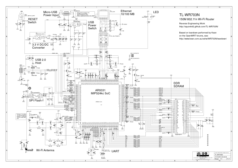
- An Atheros AR9331 chipset with
- An Atheros AR7040 400 MHz MISP24kc CPU
- Integrated 802.11n 150 Mbps (130 Mbps real) Wi-Fi with 20 dBm (100 mW) output power
- 4 MB of serial (SPI) Flash memory
- 32 MB of DDR SDRAM
- An USB 2.0 host port
- A shielded Ethernet 10/100 Mbps RJ45 jack
- An external power supply using a provided wall plug via a micro-USB socket
- A software-controlled reset pinhole switch
- A blue surface-mounted LED (that can be replaced by a 3 mm through-hole LED)
- A built-in Wi-Fi printed antenna (that can be replaced by an external one)
- An UART accessible via 2 tiny pads that provides access to the uBoot bootloader and the Linux 2.6 console
This device was released in August 2011 in China, and is not exported, though it is easy to get one on eBay.
There is also a closely related sister device as the TL-MR3020 for the export market, with the following differences:
- It is CE/FCC certified
- It has 4 additional surface-mounted LEDs
- It has an additional sliding switch with 3 positions
- The reset button is combined with the WPS LED
- It has 2 Wi-Fi printed antennas, but only one is actually used
- The RJ45 Ethernet jack is not shielded
- The UART is available on a nice 0.1” pitch through-hole connector (not mounted)
- It is larger: 67 mm x 74 mm x 22 mm)
- It is more expensive: $39 on eBay
Why?
Because of these interesting characteristics, people started to imagine unforeseen applications for this custom OpenWrt module as the cheapest available embedded Linux platform on the market, ranging from software-only firmware customization, to hardware hacks involving fine pitch soldering in order to control various physical devices.
The manufacturer is making its best efforts to comply with the requirements of the GPL license by providing access to sources releases of the modified GPL software used in the original firmware (actually, those of the related TL-MR3020 device, but they are close enough). Although not useable as is, all these modifications has been ported to several existing embedded Linux distributions, and the dedicated embedded OpenWRT distribution is an excellent choice for its easy build system and support for bleeding-edge packages.
Naturally, the ardware-focused projects using the TL-WR703N tend to be centralized in a few OpenWRT forum threads ([1], [2], [3], [4], and [5]), and rapidly focused on the research of available I/O resources and low-level electronic understanding. In this regard, the TL-WR703N router suffers from a complete lack of information reagarding its hardware implementation:
- The datasheet for the main chip (Atheros AR9331) is only available under NDA (Non-Disclosure Agreement)
- No available schematic, layout or BOM (Bill Of Materials) files
Although some progress has been made, like an almost exhaustive main AR9331 chip pinout and a component-by-component description, only a full reverse-engineering work can provide the answers to all the questions people will have on the TL-WR703N hardware.
So the goal of this reverse-engineering of the TL-WR703N router hardware is not to reproduce the device as is, as both the main chip is not available for retail, and because it would be difficult to beat the already low prices achieved by the Chinese manufacturer anyway. But the main purpose of this work is to provide the knowledge required to fully understand the hardware of this amazing little device and allow people to use it as a custom OpenWrt module for any usage you can think of.
Who?
This is the work of a single person (Squonk42), based on the TL-WR703N teardown performed by Kean from the OpenWRT forum.
Where?
All the resulting files are available in the corresponding GitHub repository, and discussions are taking place into the corresponding threads from the OpenWRT forum.
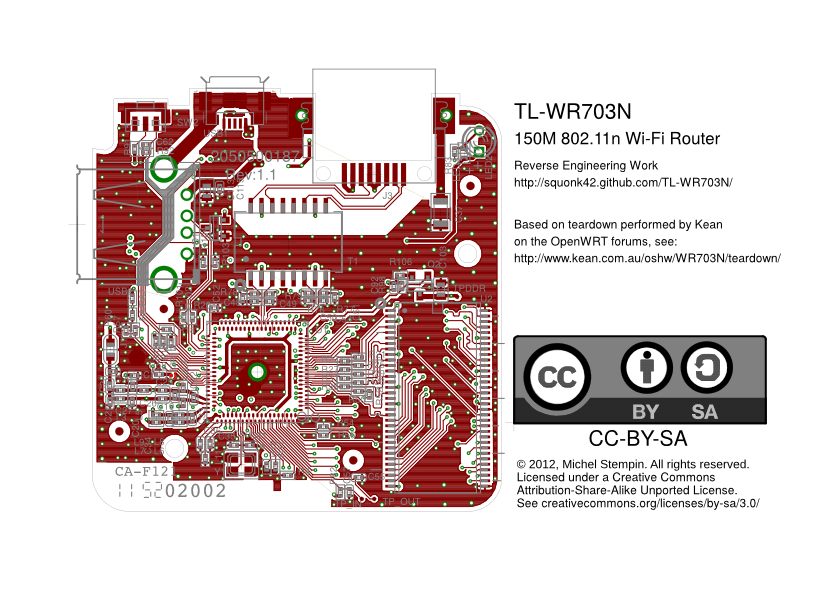
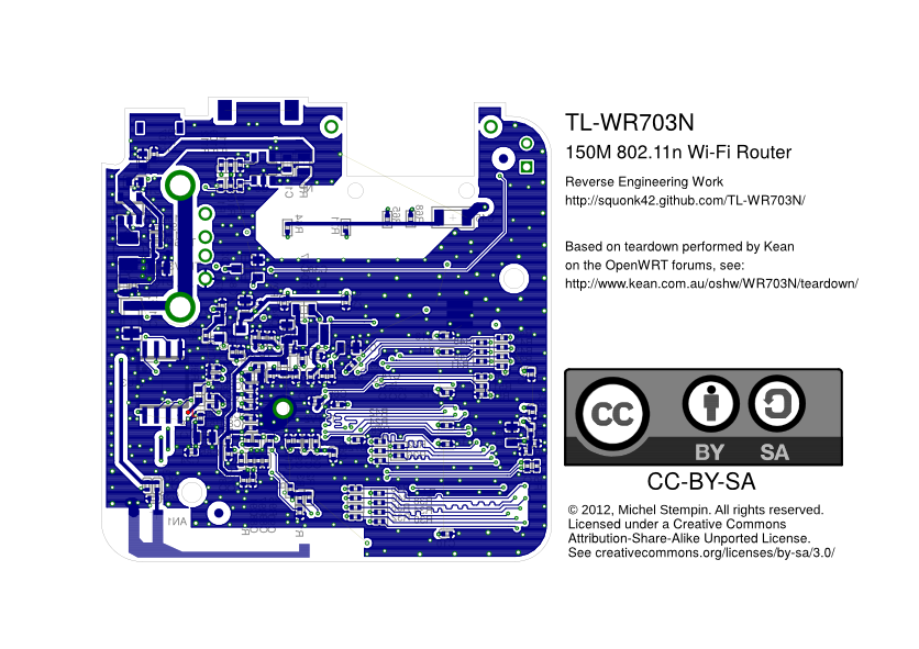
The CAD files are designed using EagleCAD v6.10. Despite the fact that the free version is limited to 2 layers only and that the boards has more layers than that, this should not be too much of a problem, as there are only a few signals located into the internal layers.
So any question, idea, remark can be posted there!
When?
This work took around 150 hours (2 week-ends and all the evenings in-between on my spare time) to produce a first PCB layout from the raw PCB top and bottom pictures.
But spare time costs nothing, and hobbyist motivation is higher than normal paid work!
How?
If I remember correctly, Kean took the PCB pictures using an 18 Mpx camera. Removing all borders and cleaning up the original pictures, this resulted into images of 3090 x 3210 pixels. As the PCB is approximately 1.9" x 1.9", the achieved resolution is something close to 1600 dpi, or a little bit better than a common 1200/2400 dpi flat bed scanner in one direction, worse in the other.
The drawback is that using a camera with a large depth of field, the image is not perfect. It contains:
- perspective (i.e. board edges are not parallel, and are not parallel either to the picture edges)
- a "barrel" effect due to the lens in macro mode
- pixels are not necessarily "square" in X and Y
- the actual scale is unknown
The first step was thus to clean up the picture using the perspective correction function of PS as a picture editing tool to straighten borders.
As for the other 2 next problems, the trick was to find something into these pictures that can be taken as a reference with known dimensions: the best guess was to take a large chip with numerous evenly-spaced pads, like the main AR9331 SoC U1 or the SDRAM chip U2. Using the same graphical editing program as used above, tools for correcting the lens "barrel" effect and scale differently in X and Y were used to get perfectly square pixels.
Now, both sides couldn't be directly superimposed: holes, vias and the PCB contour itself did not match correctly. A good way to fix this problem was to use PS's "puppet warp transform" tool with the 2 PCB sides on separate layers with transparency. This tool allowed to place and drag pins over the picture, so it could be stretched locally. Using this technique, it was possible to make both sides match perfectly by first placing pins at the 4 corners, then adding more pins as required until a perfect match was obtained.
At this point, 2 perfectly matched/square pictures with a resolution close to the original snapshots were available.
The last problem related to unknown scale required to perform a resize operation on these pictures, so they can be superimposed with the PCB in the ECAD software used (EagleCAD). Again, the same chips as above were taken as references with known dimensions. Based on the datasheets, their footprint was first created into EagleCAD with exact "real" dimensions, then placed into an empty PCB file.
As I still use Windows XP, I had to use the Glass2K utility to get either a transparent EagleCAD or picture window. Putting the EagleCAD window as large as possible on my screen, I aligned the footprint with the picture, by scaling the picture so that the round 25% picture scale was matching the EagleCAD full screen display.
By adjusting EagleCAD zoom factor from the default 1.2 to 2, it is now possible on my screen to scale the picture to 50/100/200% while zooming along with EagleCAD, and thus zoom into details "almost" easily.
That was all for the pictures, no editing any more! The drawback is that because of this last step, they are adjusted to my screen setup and cannot be shared with others easily.
The next big job was then to create all the component footprints as an EagleCAD part library. Having 2 screens helped a lot in this case, and using transparency as above, it was possible to check that the footprint was correct directly into the picture. Still, this was a tedious job. As I was doing that, I took this opportunity to also create the corresponding schematic symbols and the parts for tying the symbols and the footprints together.
Once all the parts were created, I placed them onto the PCB/picture as accurately as possible, then started to route all traces in between. There was a trick to integrate existing vias into a trace: I had to get info on the via to find its signal name, then name the trace using the same name, so they both belong to the same signal. Also, when there was only a single signal pad to connect to a via, I had to artificially add a dummy part to first create a ratsnet between 2 pads, get via info/name the ratsnest as explained, then destroy the dummy part...
I used a 1 mm/0.05 mm grid, and only a few different trace widths. However, I had to create 2 signal "classes" with different clearance values to create the correct ground/power planes.